|
|||||||||||||||||||||

|
|
|
Revised 1/2/06 |
||||||||||||||||||||||||||||||||||||||||||||||||||||||||||||||||||||||||||||||||||||||||||||||||||
|
|
||||||||||||||||||||||||||||||||||||||||||||||||||||||||||||||||||||||||||||||||||||||||||||||||||
|
The NMOS II Hybrid Microprocessor:
At first, the choice of processor architecture was initially left open. However, it didn’t take long for the processor team to zero in on HP’s 211x minicomputer architecture. Many aspects of this architecture made it the right choice but two stand out. First, it was the processor architecture used in the second-generation desktop calculators so the experienced software developers in Loveland were already familiar with the HP 211x programmer’s model. Second, HP introduced the HP 2116A minicomputer in 1966 so the HP 211x architecture was already six years old by 1972 and there was substantial software-development support for the architecture (compilers, assembler, linker, loader, debugger, etc.). There was also an existing development platform—the HP 211x minicomputer family. (Today, we call these available tools the architecture’s “ecosystem” but microprocessor marketing wasn’t that sophisticated back then.) According to Maitland, the availability of HP 211x software-development tools finally forced the issue and the choice as made. HP Loveland would again use HP’s minicomputer architecture as the base for its third-generation calculator processor.
Another feature of the HP 211x minicomputer architecture that was removed was multi-level indirection. In the HP 211x minicomputer architecture, the uppermost bit of a memory-reference instruction (the 16th bit) serves as an indirect-bit indicator. If this bit is set, then the contents of the referenced location is used as an address pointing to the location of the target address for the memory-reference instruction. If the 16th bit of the value stored at that target address is set, that address is also an indirect pointer, and the processor uses the pointer to fetch the contents of the next location in the indirect chain. Eventually, the processor finds the actual desired value. The HP 211x minicomputer’s ability to perform multiple-level indirection imposed a high cost—it reduced the processor’s addressable memory space by half, to 32 kwords (64 kbytes). That didn’t seem like much of a limitation when the HP 2116 was introduced in 1966 because back then, minicomputers all used very expensive and therefore very small read/write core memories. But it certainly would pinch the desktop calculator systems being designed in 1972. Eads looked at the operating system code written for the HP 211x minicomputers (RTE, the real-time executive) and found very few places where multi-level indirection was actually used. The feature was deleted from the hybrid microprocessor’s architecture. Deleting the multi-level indirection feature gave the hybrid microprocessor full 64-kword (128-kbyte) addressing. Even 64 kwords of memory eventually proved inadequate for the growing amount of software in HP’s desktop machines and a block-switching chip would be added to the hybrid microprocessor to further enlarge the addressable memory space for the HP 9845A desktop computer. Tom Osborne and ASM design With the architecture chosen, attention turned to the implementation, the microarchitecture of the machine. No one on the team had ever built a microprocessor, so the project was treated as more of an exercise in logic design. Nearly 10 years earlier at the University of California at Berkeley, Tom Osborne had developed a comprehensive technique for designing state machines that he called “Algorithmic State Machine” (ASM) design. In 1965, he had used ASM design to create the prototype calculator that evolved into HP’s first-generation desktop calculator, the HP 9100, which was introduced in 1969. Over the years, HP had fully embraced Osborne’s ASM design methodology. Chris Clare, a project manager in the Electronics Research Laboratory of HP Labs, started to organize and teach classes in ASM design attended by HP engineers from around the company. Clare would publish a book on ASM design in 1973 titled Designing Logic Systems Using State Machines. Tom Osborne had believed that his ASM design techniques would allow him to design anything. That same confidence infused the HP engineers in Loveland who faced the task of designing HP’s first microprocessor in 1972.
However, a big problem loomed. Dave Maitland had designed the NMOS 4-kbit ROM by himself. The three NMOS II chips that would go into the hybrid microprocessor were too large and complex to be designed by one person. However, no one at HP knew how to parcel out the design work so that several people could work on one chip together. It had not been done before. Maitland and Ed Olander did the only reasonable thing they could think of—they went fishing in the clear Wyoming lakes north of Loveland to discuss the problem in a quiet setting. And the answer is… The solution that Olander and Maitland came up with on the lakes in Wyoming was microprogramming, which was first developed by Maurice Wilkes for the EDSAC computer in 1951. Tom Osborne had essentially used it in the HP 9100’s design a few years before, although the hardware controlled by the HP 9100’s rope-memory microcode ROM didn’t really resemble the classical model of a processor. In 1972, microprogramming was hardly a new design technique, but it had not yet been used in IC design. The advantage of the microcoded-design approach for the hybrid microprocessor is that it divided the design work into two portions: the hardware design of the processor’s functional units and the programming of these functional units to implement the architecture’s machine instructions (control and timing). A small group of engineers could design the functional units and other engineers could create the microcode, which would drive control registers on the chip that caused the functional units to execute the hybrid microprocessor’s instructions. The two design groups could work in tandem, which would save time. This IC-design technique appears in the groundbreaking book Introduction to VLSI Design, written by Carver Mead and Lynn Conway and published in 1980. The “Mead and Conway” book served as the inspiration and guiding light to thousands of chip designers in the 1980s. The design technique of using a microprogram ROM to control a data path on a chip was first developed at HP in Loveland for the hybrid microprocessor. It is now a bedrock foundation of all chip design. It won’t all fit Analysis of the design task at hand by Dave Maitland and HP Loveland’s process-development engineers made it apparent rather quickly that all of the desired features wouldn’t fit on one of the new NMOS chips, unless it was a very big chip. At any given level of process development, IC-fabrication technology can economically make chips only so big. Any bigger and the defect densities on the manufactured chips drive yields to unacceptably low levels. (The larger chips will either get too expensive or impossible to make.) The early processor architectural analysis clearly indicated that some partitioning of the processor would be needed. All of the logic would not fit on one chip and yet the processor design required minimal signal-path length and capacitance so that the resulting processor design would run at high clock rates to achieve the desired performance. (Disappointing Bill Hewlett, who had been very dissatisfied with the performance of the second-generation desktop calculators, was not an option.) The processor design quickly turned to hybrid manufacturing techniques to solve the partitioning problem. The processor logic was divided into three NMOS chips: the binary processor chip (BPC), the extended math chip (EMC), and the I/O chip (IOC). These three chips would be attached and wire-bonded to a ceramic substrate that would use printed-circuit traces to interconnect the chips, creating a hybrid device that behaved as one chip. BPC, EMC, and IOC The BPC implemented 56 instructions that were considered the core HP 211x instructions. It implemented the HP 211x architecture’s two accumulators (A and B), the program counter (P), the return-stack pointer (R), six flags (including four external flags driven by inputs from other chips on the hybrid or system components outside of the hybrid), and the multilevel indirect addressing scheme. The BPC’s instructions included memory-reference, skip, alter, complement, and shift/rotate instructions. The BPC also implemented the new stack pointer required to run code from ROM.
Although the BPC alone lacked the I/O bus, advanced interrupt, and DMA capabilities planned for the hybrid microprocessor, it could reference I/O devices that were mapped into the BPC’s memory space by using memory-reference instructions from its 56-instruction repertoire. The BPC was designed so that it could be used by itself as a 16-bit microprocessor by packaging it in a more conventional ceramic DIP (dual inline package). It was used this way in the HP 9871A impact printer, which was developed by Bob Bump and Gary Paulson (introduced in 1975), the very successful HP 9872A graphics plotter (introduced in 1977), and the revolutionary HP 9874A glass-platen digitizer (introduced in 1978), which was developed by Frank Carau and Larry Brown, the electronic and mechanical engineer respectively. The HP 9871A was the first HP product to use the BPC.
The IOC implemented 12 new I/O instructions, two stack pointers (C and D), a 2-level vectored-interrupt controller, and the DMA controller. The new I/O instructions looked like the HP 211x minicomputer I/O instructions, which referenced an address space separate from memory. The HP 2116 I/O instructions had used a 6-bit I/O select code to address the 48 I/O slots available in a fully expanded HP 2116 minicomputer. The hybrid microprocessor’s I/O instructions redefined that 6-bit I/O select-code field into a 4-bit select code and a 2-bit register code. This remapping allowed desktop calculators based on the hybrid microprocessor to address as many as 16 peripheral devices (using the 4-bit select code). The 2-bit register code subdivided each peripheral select code into eight addressable 16-bit registers (four writeable control and data registers and four readable status and data registers). This new I/O scheme proved remarkably flexible. The IOC’s instructions consisted of a DMA group (five instructions), an interrupt group (two instructions), a stack group (six instructions) that used the C and D stack pointers, and an I/O group (two instructions). The IOC’s I/O instructions performed I/O through four “phantom” registers labeled R4 through R7, located in the hybrid microprocessor’s memory-address space at locations 0004 through 0007. A memory-read or -write operation directed at these memory addresses initiated I/O cycles to the specified register in the connected I/O device using the select code stored in the IOC’s peripheral address (PA) register at memory location 0009. (Note: HP generally used octal notation back in the 1970s, but the register addresses used here are hexadecimal, in recognition that octal notation is now thoroughly archaic.) The IOC employed synchronous I/O cycles—there was no hardware handshaking with the peripheral-device registers. Instead, polled I/O operations read a status register in the peripheral device (this register was always readable) to determine if data was ready (for I/O read operations) or if the peripheral device was idle (for write operations). When the peripheral device was ready, the software would perform the desired data read or write. For interrupt and DMA operations, the peripheral device would only assert the interrupt or DMA request when it was ready for the next transaction, thus effecting a handshake mechanism. The IOC’s priority-interrupt scheme was based on select code. There were 16 select codes. The upper eight select codes were assigned to the high-priority (level 2) interrupt group and the lower eight select codes belonged to the low-priority (level 1) interrupt group. Each group had its own interrupt line into the processor. When a peripheral device asserted one of the interrupt lines, the IOC performed an interrupt poll to determine the select code of the interrupting device. If more than one device in the priority group was requesting the interrupt, the device with the highest select code within the priority group was granted the interrupt. Level 2 devices could interrupt level-1 interrupt service routines because they had the higher priority level. The EMC implemented 15 instructions, mostly used for the BCD arithmetic that had become a standard part of HP Loveland’s calculators. These instructions were developed by profiling and analyzing the arithmetic routines used in the HP 9810, 9820, and 9830 to determine which instructions would most speed arithmetic computations. It was therefore quite convenient that the previous generation of desktop calculators had been based on similar processor architecture. Eleven of the EMC instructions operate on BCD-coded, 3-word (12-digit) mantissa data. A twelfth instruction performed binary 16x16-bit multiplication (using Booth’s algorithm) to produce a 32-bit result. Another instruction cleared the BPC’s decimal-carry register. The remaining two instructions implemented block-move and block-clear operations on data blocks ranging from 1 to 16 words. The IDA bus The BPC, EMC, and IOC would connect to each other over an internal 16-bit bus on the hybrid called the IDA (Instruction/Data/Address) bus that time-multiplexed instructions, addresses, and data words. Each of the three chips had its own internal controller, instruction register, and instruction decoder. In effect, the BPC fetched the next instruction for all three chips and each chip would then decode the instruction simultaneously. The chip recognizing the newly decoded instruction as its own would take over control of the IDA bus (and the rest of the processor) for the duration of that instruction. The other chips simply ignored the instruction. After executing the fetched instruction, the BPC would fetch the next instruction and the process would start over again.
Because each of the three chips (BPC, EMC, and IOC) contained its own working registers and because the other two chips might need access to the contents of a register in a third chip, all hybrid microprocessor registers were mapped into the first 32 locations in the hybrid microprocessor’s memory space. A bus-request/bus-grant handshake allowed any of the three NMOS chips to acquire control of the IDA bus and then move data across it either to another of the NMOS chips, to memory, or to a peripheral device. The bus-grant signal was daisy-chained and the IOC was first in line on the chain, so it had the highest priority for the IDA bus. (I/O requests sometimes cannot wait.) Through these mechanisms and protocols, the IDA bus moved register data among the three NMOS processor chips and throughout the system. Designing the chips With the system partitioned, work turned to designing the actual chips. Bill Eads became the project leader for the BPC and the EMC. Dave Maitland became the project leader for the IOC and the NMOS II 16-kbit ROMs that would hold the operating-system and programming-language code. Maitland eventually took over management of the entire hybrid microprocessor project. The BPC development team included project leader Bill Eads; engineers Dennis Peery, Ken Eldredge, and Wally Wahlen; and IC-layout specialist Bill Thayer, who had troubleshot circuitry as a technician on the HP 9101 Extended Memory for the HP 9100A desktop calculator. Armed with just Tom Osborne’s ASM design methodology, the BPC team designed their chip mostly by hand. Commercial EDA tools for chip design and layout simply didn’t exist back then. If the team needed a design tool, they had to create it. For example, Eads recalls that the BPC team ran a single-pass logic simulation of the BPC’s design on an HP 9820 desktop calculator. That was the extent of HP’s chip-design automation in 1972. Bill Eads moved from HP Santa Clara to Colorado and started working at HP Loveland on April 10, 1972. He worked with Olander and Maitland to define the hybrid microprocessor, formed his BPC design team, and designed the BPC. The the mask patterns were taped out on April 8, 1973 and sent to Santa Clara to make the photomasks. The HP engineers, who had never before designed a microprocessor, managed to design one in 363 days.
They had functional first-silicon chips in hand a few weeks later but a few things didn’t work right. The compare instruction was supposed to skip the next instruction if a designated value stored in memory (“compare” was a memory-reference instruction) wasn’t equal to the value stored in the designated accumulator (A or B). Instead, the first-silicon BPC skipped if the values were equal. In addition, one instruction group (possibly the shift/rotate group) didn’t decode correctly and therefore didn’t work. However, a few software patches circumvented those flaws and allowed work to progress. A second spin on the silicon produced a fully functional BPC a few months later. Each of the three NMOS II chips designed for the hybrid microprocessor came out roughly the same size: approximately 4.7mm on a side. Each chip incorporated a microcode ROM containing approximately 8000 bits and, on average, 6000 transistors (2000 equivalent gates) to implement the logic circuits. The chips used four power supplies (5, 7, 12, and -5V) and could run at clock rates exceeding 10 MHz. There were also four small bipolar ICs on the hybrid microprocessor. Theses chips were called BIBs (bidirectional interface buffers). The 8-bit BIBs provided voltage-level translation between the NMOS BPC, EMC, and IOC chips on the hybrid processor and the bipolar logic in the rest of the calculator system. The BIBs also provided the low-impedance signal-driving ability that was needed to drive the memory and I/O busses throughout the rest of the calculator system, beyond the enclosed world of the hybrid microprocessor. Two BIBs buffered the NMOS processor chips from the memory bus and two more BIBs buffered the I/O bus. Like the NMOS chips, the bipolar BIBs were made in Loveland.
Rubber baby buggy bumpers
When the heat-sink/ceramic-hybrid assembly was bolted to the circuit board, the elastomeric connectors were sandwiched between the ceramic substrate and the circuit board. Assembly took less than a minute, everything fit within tolerances, and the connections were made between the processor and circuit board quickly and reliably. It was a simple, elegant, and relatively cheap solution to a number of complicated engineering problems.
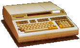
Various versions of HP’s 16-bit hybrid microprocessor served as the heart of several desktop computers including the HP 9825A/B, HP 9831A, HP 9835A/B, and HP 9845A/B/C. Ed Miller wrote a data book and manual about the hybrid Microprocessor. It was called the “How They Do Dat Manual” and it was illustrated by HP Loveland’s in-house engineer and cartoonist Rand Renfroe. The documentation allowed other HP divisions to use the hybrid microprocessor in their own products. HP’s Santa Rosa Division used the hybrid microprocessor as the heart of its HP 8566A and 8568A spectrum analyzers. In fact, development of the HP 8566A and 8568A started before the first hybrid processor was made, so the early prototypes of these analyzers used an HP 2100A minicomputer as the control processor. The engineers at HP Santa Rosa, in particular Lynn Wheelright, had a preference for Algol, a structured high-level language that was popular in the 1970s. Wheelright developed a compiler for the hybrid microprocessor as well, an an Algol variant that he dubbed “Wheelgol.” HP owned up to programming the spectrum analyzers in Algol, but kept the name “Wheelgol” under wraps. Later, when the HP 8566A and 8568A spectrum analyzer designs migrated to the Motorola 68000 microprocessor, Wheelright found it very easy to change the compiler’s back end to target the newer microprocessor. HP’s Colorado Springs Division also used the hybrid microprocessor (minus the EMC) in various incarnations of its HP 64000A Logic Development System, a microprocessor development system and in-circuit emulator used to develop embedded software for a number of different microprocessors including Intel’s 8086, Zilog’s Z80, and Motorola’s MC68000. In all, HP sold products based on HP Loveland’s hybrid microprocessor and its constituent chips (BPC, EMC, and IOC) for more than a decade. Quite a track record for the world’s first 16-bit microprocessor, which very few people had ever heard of, until now.
Problems in production Dodging the floppy When Shaffer arrived at HP Loveland in July, 1976, it first looked as though he'd be going into production engineering along with the HP 9885 floppy disk drive. The drive had been designed by Sandy Chumbley, who had started with HP as a technician but grew into the roles of engineer and, eventually, manager. Chumbley had hosted Shaffer during his initial HP interview and was responsible for giving Shaffer his first assignment. Designing a better tester On his first visit to the production area, Shaffer found that the hybrid microprocessor tester essentially consisted of an entire HP 9825 desktop calculator with a hole cut in it so that hybrid processors to be tested could be dropped into place. This tester had been built by an engineer named Joe Fucetola. Essentially, the production test for the hybrid microprocessor consisted of clamping the processor in place and seeing if the calculator would power up correctly. If it did, the hybrid processor must be operable. Otherwise it was bad. Unfortunately, this sort of go/no-go test doesn't provide much in the way of diagnostic information, which is required for developing a mature production process. In addition, the physical configuration of the tester prevented the probing of signals on the hybrid microprocessor during the test, further inhibiting failure analysis.
Dyke wrote: “This is the only picture I remember taking of the two BPC hybrid testers as they were in production for the last 10 years of the run of bpc hybrids in Fort Collins. It was the culmination of 2 years of work from redesign of the ceramic substrates thru the wire wrap version of the tester to these two fully featured versions with their 14 pcb assemblies and industrial design that I did to facilitate manufacturing test, debug and functional test.” Follow the bouncing ground These experiences transformed Shaffer into HP’s resident expert on the operation and testing of the hybrid microprocessor and he next tackled another, intermittently occurring problem with the microprocessor. The problem was a signal glitch that appeared on the hybrid's control signals. This glitch was synchronized to transitions on the processor’s main address/data buses. The cause of the problem turned out to be ground bounce.
As the resident expert on the hybrid microprocessor, Shafffer also expanded his work into software. He wrote a binary program for the HP 9825 that, among other things, implemented an incremental assembler for the hybrid microprocessor’s instruction set and a set of commands to build and access symbol tables, perform arbitrary base conversion between numeric and string variables, and numerous other utility commands that were used during the development and deployment of other electronic tools used during the production lifetime of HP’s 98x5 series of desktop computers. In 1983, Shaffer moved to HP’s Santa Rosa Division in California and finally got back to the analog and RF work that had originally attracted him to electrical engineering. But he never left his digital experiences in Colorado far behind.
|
||||||||||||||||||||||||||||||||||||||||||||||||||||||||||||||||||||||||||||||||||||||||||||||||||


|
| [Home] [Prehistoric Times] [The 9100 Project] [Prologues] [The 9825 Projects] [Epilogues] |