|
HP’s introduction of the HP 9100A programmable desktop calculator in 1968 opened big, new markets for Hewlett-Packard. One of those was the scientific/engineering calculator market. Engineers and scientists have always needed to crunch a lot of numbers in their work and programmable calculators are very handy tools for making such computations. The other market addressed by the HP 9100A was that of the instrument-control market, the same market that had finally enticed Bill Hewlett to permit HP’s foray into minicomputers. The HP 9100A substantially dropped the cost and size of an instrument controller and many people started to use it as a controller for operating sophisticated data-acquisition systems. HP 9100 users quickly outstripped the additional memory of the enhanced HP 9100B (introduced in 1969) and of the HP 9101 external-memory add-on box. Consequently, by 1969, the calculator engineers at HP’s Loveland Division were already starting to consider how they would follow up their first smashing success.
However, when the engineering team at HP looked at the HP 9100 calculator with an eye towards building a next-generation product, they saw Tom Osborne’s brainchild with new eyes. Osborne’s sparse and elegant hardware design tailored everything for reliability and manufacturing economy and nothing for expansion. For example, the HP 9100’s program counter (and therefore its program ROM address space) was just large enough for the existing ROM so the calculator’s firmware could get no bigger. The address space for read/write core memory was likewise limited and had already been expended through an ingenious but slightly awkward block switching mechanism to accommodate the memory expansion in the HP 9100B. A keystroke prefix was added to address the extra memory in the HP 9100B and even more key sequences had been added to further accommodate the HP 9101’s expansion memory, which could only be used as a backing store and could not be used like the calculator’s internal user memory. In short, the HP 9100 was very much a product of the transistor generation and was limited by the efficiency of its design. Every attempt to optimize for economy had placed real constraints on the machine’s extensibility. The HP 9100 hardware design would not scale easily.
Adaptation of a Minicomputer
At the same time, HP in California had developed a minicomputer architecture that might, with great engineering effort, be pressed into service as a platform for a next-generation desktop calculator. This architecture (often called a 16-bit “stretch” version of DEC’s 8-bit PDP-8 minicomputer architecture) first appeared in HP’s 2116A minicomputer, which was introduced in 1966. By 1968, HP’s Cupertino Division had developed a cost-reduced version of the machine called the HP 2114A. Studies by Ed Olander and Fred Wenninger in Loveland indicated that the HP minicomputer architecture could be adapted for use in desktop calculators.
Adapting the processor architecture from HP’s minicomputer family for a desktop calculator provided additional benefits to the Loveland Division’s calculator team besides avoiding the reinvention of the wheel. First, there were several software-development tools available for the architecture in the form of assemblers, linkers, loaders, debuggers, and compilers. The HP 9100 calculator’s only software-development tool had been a pad of paper. Second, although it ultimately turned out to be an irrelevant advantage, system software in the form of operating systems and I/O drivers had been written for the HP minicomputer family and this software could have been repurposed for a desktop calculator. In the end, this repurposing didn’t happen but it nevertheless played a role in choosing a processor architecture for HP Loveland’s next-generation desktop calculator.
It’s not that the HP 9100 hardware design could not be scaled. It could. However, doing so would have required substantial design work and the result would be a scaled up calculator that would itself not be scalable for following generations. In addition, the HP 9100 was very much a product of the transistor era and the electronics industry was already entering the next era: the era of integrated circuits. Consequently, the Loveland design team chose HP’s existing minicomputer architecture for its new desktop calculator. This decision set the course of HP’s soon-to-be-created Calculator Products Division for the next decade.
One of the major reasons for wanting a programmable processor with a complete set of software-development tools for the next-generation calculator was because the HP design team wanted to create not just one new machine but an entire family of desktop calculators to replace the HP 9100. Initially, this family consisted of three calculators but a fourth would be added eventually. At the low end would be a machine to directly replace the HP 9100, but at a lower price. This machine would replicate the HP 9100’s key-based calculator programming language, three-line numeric display, and magnetic-card reader/writer.
More of Everything, Please
However, the huge success of the HP 9100’s programming features and the customers’ constant cry for “more” strongly indicated that there was an untapped market for desktop calculators with even more powerful programming features. Thus the Loveland engineers defined mid-range and high-end desktop calculators in addition to the low-end model that would replace the HP 9100. All three of the new-generation machines would share a common hardware core including the processor and the I/O structure and several case parts. However, key internal peripherals including the keyboard, display, printer, and mass-storage device would vary from one machine to the next as would the amount of memory (ROM and RAM) installed in each machine.
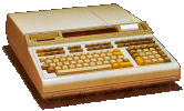
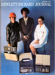
The three machines defined in this new series of calculators would be named the HP 9810A, 9820A and 9830A. Collectively, these second-generation machines were known as the HP 9800 series. The HP 9810A was a key-per-function machine employing reverse-Polish notation, like the HP 9100. It had a three-line, numeric display like the HP 9100 but it used a numeric LED displays to show register contents instead of the HP 9100’s CRT, which permitted the HP 9810A to have a smaller form factor and eliminated the expense and heat of the CRT’s high-voltage power supply. Like the HP 9100, the HP 9810A also had a magnetic-card reader/writer for storing user programs and data.
The HP 9820A employed a more computer-like algebraic user programming language, which would eventually be named HPL for “high-performance language.” It had a one-line alphanumeric LED display and a magnetic-card reader/writer. HPL would subsequently grow into the language implemented in the HP 9825A and B desktop computers, to which this Web site is dedicated.
Finally, at the top of the line, the HP 9830A had a wider, more capable one-line alphanumeric LED display than the HP 9820A. The HP 9830 also used a digital version of the Philips Compact Cassette tape drive for mass storage, which provided substantially more storage capacity, commensurate with the HP 9830’s needs because this top-of-the-line member of the original 9800 family ran a relatively new programming language called BASIC, the Beginners All-purpose Symbolic Instruction Code. BASIC was developed by Kemeny and Kurtz at Dartmouth College and would become the early user-programming language of choice for microcomputers in the mid 1970s, thanks to a Harvard student named William Gates III who would go on to build his company, Microsoft, into the world’s largest software vendor. But at this point in the story, that’s Microsoft Basic is still five years in the future.
Even though the processor architecture chosen for the HP 9800 series had already been implemented in the HP 2114A minicomputer, HP’s calculator engineers faced many problems in building a desktop calculator based on that existing architecture. First, and perhaps most important, was system cost. The already “cost-reduced” HP 2114A with a teleprinter cost $15,950 in 1969, a price that compared very poorly to the existing $4900 HP 9100B desktop calculator. In fact, HP Loveland wanted to produce a next-generation replacement that cost less than the HP 9100 calculator, to broaden the available market and to make room at the high end for more capable (and more expensive) desktop machines like the HP 9830A. So the Loveland designers had a lot of cost reducing ahead of them and they attacked this problem at the points of commonality among all of the HP 9800 series calculators: the processor, memory and I/O.
First of all, the HP minicomputer architecture was implemented with several large boards connected with several wide, parallel buses. This design approach used a lot of hardware and incurred a lot of manufacturing cost.
Second, the existing HP 2114A minicomputer architecture used magnetic-core memory to store the machine’s operating system, programming language, user program, and user data. That’s because 1960s-era minicomputers traditionally relied on an attached mass storage device to supply the stored user code and data when needed. Often this mass storage was either a very slow paper-tape reader or a very expensive hard-disk drive. HP’s existing HP 9100 calculator customers were already accustomed to throwing the power switch and having a fully operational machine only seconds later, so they wouldn’t tolerate the glacially slow time it took a minicomputer to load an operating system from a paper-tape reader and they couldn’t afford to buy a hard disk for every calculator because such hardware was prohibitively expensive in 1970.
To achieve a fast boot time in the new generation of calculators, the Loveland engineers planned to install the calculators’ operating software and programming languages into fast semiconductor ROM, which worked like the HP 9100’s pc-board ROM but provided more capacity at less cost and in less space. Similarly, they would put the user program and user data, which required read/write memory, into semiconductor RAM instead of the HP 9100’s very expensive core memory.
Because the HP 9100’s pc-board ROM in its existing form was already labor-intensive and expensive, and because would not scale either economically or technically to the much larger sizes needed by the new calculators, and because commercial semiconductor ROM and RAM chips had not yet evolved to the required storage capacities, HP had to make a big decision. To use such large semiconductor ROMs and RAMs, the company would have to fabricate them itself, which would require that HP’s Loveland Division develop the in-house ability to make large digital integrated circuits.
At this point, you should be reminded that Loveland, Colorado was an isolated center of high-technology in the late 1960s, quite apart from Silicon Valley’s exploding semiconductor scene. However, developing the in-house ability to fabricate advanced-technology components of all types was a defining characteristic of HP in those days and the calculator engineers relished the challenge even though they all thought it was quite risky. The decision to develop the in-house ability to fabricate large-scale digital ICs would trigger HP’s development of several generations of high-performance NMOS memories and sophisticated microprocessors over the next 30 years. Echoes of this decision, which was made in 1970, still faintly reverberate in the design of the Itanium processor, jointly developed by HP and Intel.
Finally, the rack-mounted HP 2114 minicomputer’s form factor for I/O cards, derived from the original design for the HP 2116A instrumentation minicomputer’s I/O cards, was simply too large for the more diminutive desktop calculators. Yet the desktop calculator’s growing role as an instrumentation controller mandated that the HP 9800 series of desktop calculators have excellent I/O capabilities. Note that the original HP 9100 did not have excellent I/O capabilities. In fact, the HP 9100 got its I/O abilities by accident through a test connector because its original intended purpose was as a calculator, not an instrument controller.
However, customer desire to use the HP 9100 as an instrument controller was so great that HP engineers (and even some very determined customers) found ways to expand the HP 9100’s I/O abilities in spite of its I/O limitations. For the new 9800 series calculators, the Loveland engineers would develop a new I/O scheme. This new scheme would be purpose-built for peripheral and instrument control. As a consequence of the decision to develop these I/O capabilities, the evolving families of HP desktop calculators and computers would dominate the instrument-control market well into the 1980s, when the mantle would finally be passed on to the IBM PC and its myriad lower-cost descendants.
The above three problems are the classic ones that haunt any new computer design because they directly relate to the component trinity of computer-system design: processor, memory, and I/O. Together, those three basic building blocks determine the overall performance of any computer system. When all three are in balance in terms of speed and capacity, the system design is in balance and the system will perform optimally. If any of the three is not in balance with the others, the component with the lowest performance or capacity determines the overall system performance by placing a drag on the performance of the other two system components.
Too Much Work for One Division: CPD and LID
The adaptation of HP’s minicomputer processor architecture to the desktop form factor, the development of three new and very different desktop calculators, and the development of a new digital IC process technology to support these plans represented a huge amount of engineering work. HP was willing to underwrite this endeavor because sales of the HP 9100 desktop calculator and its peripherals were generating a lot of cash and indicated the presence of a large, untapped market for HP. However, HP was not willing to burden an existing division with such a large undertaking because it might divert that division’s attention away from existing, successful product lines. The time had come to create a new HP division devoted to this new market.
And so Don Schulz found himself in a meeting in 1970 with Bill Hewlett and Marco Negrete, who by now was General Manager of the Loveland Division. Schulz had become HP’s first lab section manager back in Palo Alto and had moved to Colorado with Chuck Near to transform the HP 9100 prototype, which had been developed in Barney Oliver’s Palo Alto R&D lab, into a production machine. At HP in those days, promotion to section manager was the stepping stone to becoming a division lab manager. Schulz had already seen many people who became section managers after him promoted to lab manager in California and Schulz felt ready to do the same. He was quite eager to hear about plans for a new division, which would naturally need a new lab manager.
Hewlett and Negrete explained to Schulz that the time had indeed come to split calculators off from the Loveland instrument operation. They then questioned Schulz about Bob Watson, who had worked as a manager under Schulz on the HP 9100 project. Schulz, assuming that Hewlett and Negrete were asking questions about the person they planned to put in Schulz’s place as section manager when they promoted Schulz to calculator lab manager, extolled Watson’s virtues and accomplishments. When he was done, Hewlett nodded and said that Schulz had confirmed what he’d already heard.
However, Hewlett’s next statement shocked Schulz. Instead of making Watson a section manager under Schulz, Hewlett planned to make Watson the lab manager in the new Calculator Products Division (CPD). Watson would work for a new CPD division manager, Tom Kelly, who had been the Loveland Division’s marketing manager.
When Schulz heard these plans, he felt shocked and his vision blurred. It seemed he was to be denied promotion to lab manager yet again. Schulz abruptly rose and left the room, preferring to cut the meeting short rather than have Hewlett and Negrete see him break down. However, he heard Hewlett call out, “Don! Come back. I haven’t dismissed you yet.”
When Schulz returned, Hewlett gave him the rest of the news. The instrument operation in Loveland would be renamed the Loveland Instrument Division (LID). The existing instrument lab manager, Dick Moore, would keep his job but Negrete was leaving his position as division manager because the Loveland facility would be hosting two major divisions. Negrete would become the Loveland facility General Manager. That left the position of LID division manager open. Perhaps, wondered Hewlett, Shulz might like that position. When your name’s on the company like Hewlett’s, you can have your little fun with the employees.
And so Don Schulz, HP’s first-ever section manager, who had waited years to become a lab manager, would never hold that position because he was promoted straight into the division manager slot at LID while Kelly and Watson went off to build CPD and to solve the problems associated with creating the second generation of HP’s desktop calculators.
Problem 1: Reduce the processor’s cost
The HP 2114A minicomputer’s 16-bit processor occupied multiple cards connected by multiple, wide buses. This approach produced a faster machine at the cost of several circuit cards, many card connectors, and a lot of expensive slot-to-slot busing. This design approach was far too expensive for the next-generation calculators. The calculator designers, using a classic engineering approach to trade off cost and speed, elected to serialize the processor architecture (especially the internal processor buses), which reduced the amount of busing. This design approach, which reduced the processor’s processing width from 16 to 1 bit and substantially lowered the processor’s cost. It also resulted in a processor that unsurprisingly ran much slower than the same architecture implemented with a parallel design in the HP 2114A minicomputer.
To partially compensate for the reduced operating speed of the serialized architecture, the designers of the HP 9800 series processor added circuitry for digit-serial (instead of bit-serial) BCD computation. (The HP 9800 processor ALU could therefore operate either on 1-bit values or 4-bit BCD digits.) To implement this feature, they added new microcoded machine instructions for floating-point BCD computations that had not existed in the minicomputer’s instruction set. As calculators, all the 9800 series machines would perform a lot of floating-point math that minicomputers didn’t always need to do. In fact, early minicomputers often had poor floating-point performance because they lacked floating-point co-processors. As descendents of Tom Osborne’s HP 9100 calculator, the 9800 series calculators would provide the same numeric results as the HP 9100 by executing computations using the same BCD arithmetic employed in the HP 9100’s design rather than the more common (but less precise at the time) binary arithmetic.
The BCD architectural additions boosted the speed of the HP 9800 series processor but the second-generation desktop calculators with their serialized 8-MHz processors could not match the blazing computational speed of Tom Osborne’s original 64-bit parallel VLIW machine in the HP 9100, a flaw that HP Labs director Barney Oliver continued to bemoan two and a half decades later. (The third generation of desktop machines that followed the HP 98x0 series desktop calculators would eventually overcome that problem using a parallel, 16-bit implementation of HP’s minicomputer architecture.)
Chuck Near, who had developed the HP 9100 production testing system using an HP minicomputer, created the serialized version of the HP 2114A processor for HP’s second-generation desktop calculators. Near was assisted on the processor’s logic design by Fred Gross, Jerry Reynolds, and Gary Egan. Henry Kohoutek, a Czech-born engineer who joined HP in 1969, developed and then shoehorned all 75 of the 9800-series processor instructions into 256 28-bit microcode states that fit into seven 256x4-bit bipolar ROMs. (The 4-kbit NMOS ROM, which was being developed at HP Loveland in parallel with the other components of the 9800 series machines, was too slow to hold the 8-MHz processor’s microcode but fast enough to hold the operating-system firmware.) Two more 256x4-bit bipolar ROMs were used to implement the processor’s ALU functions in a 2-level lookup table. After finishing the 9800 series processor, Near took over the newly formed peripherals group within CPD.
Problem 2: Develop the necessary IC technology
By the end of the 1960s, commercial IC technology was really starting to ramp up and bipolar ICs were far ahead of the various MOS IC technologies. In particular, Texas Instruments’ expanding 7400 series of small- and medium-scale integrated circuits (SSI and MSI), based on bipolar technology, were becoming the industry standard for fundamental digital building blocks and would remain so into the 1980s when PALs, CPLDs, and FPGAs would take over. However, bipolar IC technology scales poorly due to its high power dissipation so by the end of the 1960s, it was clear that large-scale integration (LSI) would require development of lower-powered MOS ICs.
Marco Negrete had recognized that his growth plans for Loveland would likely require the extra abilities realized through semiconductor manufacturing. Negrete found and hired Ed Shideler to start up an IC facility in Loveland’s new building B. Shideler had worked at Fairchild and Transitron, so he had commercial semiconductor fabrication experience. He assembled a team of design engineers, process engineers, packaging engineers, and a couple of summer students to put a bipolar semiconductor fab together at Loveland.
One of the engineers he recruited was Larry Lopp, who had worked under group leader Bob Watson in the Loveland R&D lab. Lopp had been the project manager on the HP 3420A DC differential voltmeter and he had designed the circuitry for that product, but he found that circuit design just didn’t excite him. So he took the opportunity offered by Shideler to help start an IC fab in Loveland.
The Loveland lab’s early developments involved bipolar IC designs and thin-film devices such as laser-trimmed resistor networks and microwave devices. Lopp remembers traveling to HP’s facilities in California about one week in each month for a while, picking up “a lot of disconnected pieces” of IC-fabrication knowledge at HP’s Frequency and Time Division, the HP Santa Clara IC fab, and Barney Oliver’s HP Labs. “We were totally unrepentant thieves.” recalls Lopp.
The inevitable move to higher integration levels, experienced by any IC fab, occurred in Loveland as well. Lopp started by looking at PMOS, the high-density process of the day, but soon realized that PMOS circuits would be too slow to meet HP Loveland’s goals. The answer to this problem in the form of a 4-page paper came sailing over a bookshelf one day from fellow engineer Virgil Laing. “Look at this.” said Laing. The paper detailed IBM’s efforts in developing an NMOS IC process. Lopp read the paper and said, “We can do this.”
Most likely, Laing got that paper from Dave Maitland, who had been spending the year following the end of the HP 9100 development project researching IC fabrication technology at Bob Watson’s request. Watson had recognized that the next generation of desktop calculators would need bigger ROMs than the one used in the HP 9100 to accommodate more complex programming languages and more features. Watson also realized that the HP 9100’s pc-board ROM was a dead-end technology. It could not be made bigger technically and was already too expensive to manufacture due to poor circuit-board yields and the need to hand-select transistors for the pc-board ROM’s sense amplifiers. Integrated-circuit ROMs appeared to be a much better alternative. Maitland had worked on the HP 9100’s pc-board ROM so he was a good choice for this investigative work. He was highly motivated to find a better technological alternative.
Maitland’s IC research took him to the IEEE’s International Solid State Circuits Conference (ISSCC), held in Philadelphia in 1969. He freely admits that he knew virtually nothing about making integrated circuits at the time and consequently, he found many of the conference papers difficult to understand. So he made a point of sitting in the audience with IBM attendees who seemed to understand much more of the discussion and who were happy to explain things to the uninformed engineer from HP. Such were the early days of chip fabrication.
One of the papers presented at ISSCC in 1969 was a 4-page paper comparing the performance of n-channel and p-channel IGFETS (insulated-gate FETs, the old name for MOSFETs). The paper was written by four IBM engineers and it clearly discussed the advantages of NMOS (n-channel MOS) and the pitfalls in making NMOS transistors.
NMOS versus PMOS
There are two types of MOS transistor: NMOS and PMOS. Early MOS IC developments focused on creating LSI chips that used either all NMOS or all PMOS devices. (CMOS, which employs both NMOS and PMOS transistors, came later.) PMOS ICs devices were developed before NMOS ICs because they were easier to make. Ionic contamination poisons NMOS transistors and prevents them from switching off. Ionic contamination doesn’t affect PMOS transistors in quite the same way because they use holes instead of electrons to carry current. Although ionic contamination does affect the gate threshold voltage in PMOS transistors, the effect is not as severe as it is for NMOS transistors.
However, PMOS ICs have two major liabilities. They are relatively slow because they rely on lower-mobility holes to carry current instead of electrons. In addition, PMOS ICs don’t interface quite easily with the 7400-series TTL building blocks that were taking the electronics industry by storm.
Spurred by the very brief IBM paper presented at ISSCC in 1969, the IC-development group in Loveland elected to develop NMOS IC technology to get the speed and easy interfacing offered by NMOS circuits. Engineers at HP Labs in Palo Alto had been experimenting with NMOS technology and had developed some test devices. HP Loveland decided to start by trying to replicate the HP Labs technology.
Tom Ligon, who had troubleshot the manufacturing-yield problems with the HP 9100’s printed-circuit ROM board, was the first engineer on the NMOS project. He obtained photo masks from HP Labs and tried to replicate the test devices. None of the NMOS test transistors fabricated in Colorado would work. They were all dead. Ligon’s analysis of the problem showed that NMOS fabrication processes had to be at least an order of magnitude cleaner than bipolar processing to produce working devices because the NMOS gate oxide was being contaminated with ions in the etching chemicals. Better cleaning procedures removed the contaminants and working test devices started to appear. (Ligon quit HP in 1970 and set out to start his own business. However, he returned 20 months later to start work on the NMOS II fabrication process, which became one of the key, core technologies of the HP 9825 desktop computer.)
By 1970, the Loveland fab was making enough good NMOS ICs and had characterized enough of these parts so that Maitland was able to write an article about NMOS that appeared in the December, 1970 issue of Electronics magazine. However, NMOS technology remained uncommon in the semiconductor industry, as shown by its mere mention in a large roundup article written by GE engineer Herman Schmid that appeared in the December, 1972 issue of IEEE Transactions on Manufacturing Technology. Although it cites Maitland’s 1970 article in Electronics, Schmid’s article does not discusses NMOS fabrication in detail but it does cover PMOS and even CMOS fabrication extensively.
The first ICs to be made using HP Loveland’s new NMOS process were to be memories and the project manager for the 9810 memory system was Geoff Chance, who had developed The Link, a box that substantially enhanced the I/O abilities of the HP 9100 calculator. Because he was in charge of the memory system, which would be used in the first of the HP 9800 series calculators, Chance was very involved with the IC development work in Loveland. His memory system relied on getting working NMOS memory ICs from Shideler’s operation. Chance also worked with several other managers and engineers at HP on IC development including CPD lab manager Bob Watson, Calvin (Cal) Finn and Tom Haswell. Finn had been a well-regarded professor of electrical engineering at Colorado State University in Fort Collins, Colorado (located just a few miles north of Loveland) and joined HP in 1969. Haswell joined HP in 1970.
Haswell’s job was to find a way to make NMOS a practical, manufacturable IC technology. Although Ligon’s work had reduced the problems of initial FET poisoning during fabrication, sodium contamination continued to plague the NMOS process. Sodium atoms, an ever-present contaminant, poison and disable NMOS transistors by riding the electric fields inside the IC and coming to rest in the MOS transistor gates, altering the transistor gate thresholds so that the NMOS transistors often failed to work. Haswell eventually succeeded by specifying purer raw materials (especially aluminum for the interconnect) and by adding a back-gate bias voltage that provided an antidote to the sodium poisoning by making the NMOS gate threshold voltage large enough. Although the NMOS transistors were still somewhat poisoned, the back-gate bias countered the effects of the sodium contaminants. (Back-gate bias remained the industry’s solution to sodium gate poisoning until the development of ion implantation.) Haswell eventually took over as Loveland’s IC manager from Shideler and he would eventually replace Watson as CPD’s lab manager.
Haswell’s success in developing a production-ready NMOS process led to HP’s development of the industry’s first 4-kbit IC ROM, designed by Dave Maitland, who had settled into the task of developing design rules for the new NMOS fabrication process.
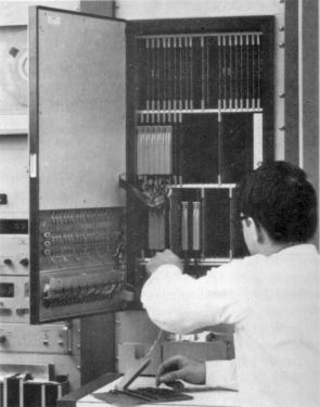
Bit patterns for Maitland’s 4-kbit (0.5-kbyte) NMOS ROMs were sent over phone lines via a teletype’s paper-tape reader and a 110-baud modem to an engineer named Bill Eads in HP’s mask shop in Santa Clara, California, where HP had built a larger IC facility. HP had gotten into the semiconductor business a few years earlier to develop its own transistors and diodes and the IC photomask shop in California had a pool-table sized coordinatograph that could cut the large Rubylith patterns on Mylar plastic that were needed to make the ROMs. ROM masks were shipped back to Loveland where the ROMs were fabricated. Eads would eventually develop a computer program to speed the production of ROM masks. Later, in 1972, he moved to Colorado to work in the Calculator Products Division.
The minimum feature size on these first NMOS chips was about 7 μm, which is roughly 100 times larger than the linear dimension of the smallest features of most advanced ICs that can be built in 2005. That means that the transistors consumed roughly 10,000 times more silicon area (100 times 100) back then than they do in 2005.
More NMOS than anyone else
The HP 9800 series calculators would have a voracious appetite for ROMs so the HP Loveland NMOS fab quickly became the world’s largest NMOS production facility. The HP 9810A calculator, with the smallest code requirements in the initial HP 9800 series, had 5 to 11 kbytes of code in ROM (depending on its installed complement of option ROMs). The HP 9820A had 8 to 14 kbytes of code in ROM and the HP 9830A had 15 to 31 kbytes of code in ROM. When Tom Osborne later wrote about the development of the HP 9800 series, he quoted an unnamed HP engineer who said, “If you think it takes nerves of steel to release a software operating system, imagine how it feels to release one in firmware.” Motorola’s semiconductor division eventually served as a second source for HP’s NMOS ROMs and, as a result, Motorola was one of the first commercial semiconductor vendors to master the NMOS process, with HP’s help.
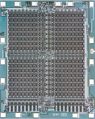
A parallel development program in Loveland for a 1-kbit NMOS RAM was progressing when HP discovered that a small semiconductor startup company named Intel in the San Francisco Bay area had announced a 1-kbit PMOS DRAM. Chance, Watson, and Shideler flew out to Santa Clara to meet and visit with cofounders Gordon Moore and Robert Noyce, who had just left Fairchild Semiconductor and had founded Intel to focus on LSI semiconductor memories. The HP engineers flew from Colorado to California to review Intel’s first 1-kbit MOS DRAM design, the 1102, which was developed as a custom product for Honeywell’s mainframe business.
As Chance recalls, Intel’s 1102 had poor reliability and a very small schmoo (engineer-speak for operating-voltage and -temperature range). Even so, Intel decided to develop the 1102 into a commercial product and HP’s calculator engineers, who wanted a similar but more robust product for the 9800 series calculators, contributed what they were learning about IC fabrication technology from their 4-kbit ROM project to help improve the Intel DRAM’s reliability and to give it a bigger schmoo.
These efforts produced Intel’s 1103 1-kbit PMOS DRAM, which was the world’s first commercially available DRAM IC and a very successful product for Intel. In fact, people at HP like to say that HP’s volume purchases of 1103 DRAMs for the second-generation desktop calculators allowed Intel to build its first expansion wing onto its facility in Santa Clara. The 1103 DRAM, formally introduced in October of 1970, was Intel’s first blockbuster product. This one device secured fledgling Intel’s future. In 1972, practically all of Intel’s revenue, $23.4 million, came from sales of the 1103 DRAM.
Inappropriate I/O
When the HP 9800 processor team implemented the HP 2116 minicomputer architecture, they removed the I/O instructions because the serial nature of the HP 9800 processor meant that HP’s existing minicomputer I/O scheme was wholly inappropriate for desktop calculators. HP minicomputer I/O instructions employed a 6-bit field that specified one of as many as 64 I/O slots in the minicomputer’s backplane. However, it was physically impossible to put 64 slots into the diminutive desktop calculators. In addition, there really wasn’t room in the HP 9800 processor’s microcode ROM for the I/O instructions.
However, the ability to interface HP’s calculators to a wide variety conventional computer peripherals (such as printers, paper-tape punches and readers, magnetic tape drives, and card readers) and more unconventional instruments (such as digital voltmeters, counters, programmable power supplies) was an increasingly important goal for the Series 9800 calculators. Consider this paragraph taken from HP’s 1973 catalog, which appeared after the HP 9810A, 9820A, and 9830A were introduced:
Consequently, a separate team under project leader Gary Egan developed an I/O coprocessor (actually more of a simple state machine) that implemented special HP 9800 versions of the I/O instructions.
The HP 9800 series calculators divided their peripherals into two types, internal and external, and the 9800 series processor addressed these peripherals differently. Internal peripherals such as the keyboard, LED displays and keyboard indicators, internal thermal printer, and magnetic-card reader/writer were directly addressed using the 6-bit slot identifier in the existing minicomputer I/O instructions. However, the external peripherals, which were connected to the calculator using special I/O cards, were indirectly addressed using a different addressing scheme.
A special I/O register, one of the calculator’s directly addressed internal peripherals, accepted 16-bit command words formed by the 9800-series processor. For external peripherals, the four most significant bits of this command word specified an external I/O slot code. The next four bits formed a status field. The lower 8 bits of the I/O register held an 8-bit output value. If the I/O command was directed at an internal peripheral, the 9800 series processor used direct addressing and the entire word in the internal I/O register could hold a 16-bit output value. If the I/O command specified an input operation, the external I/O card would return a 12-bit value consisting of a 4-bit status field and an 8-bit data field.
The entire I/O processor was implemented as a state machine that ran independently of the 9800 series processor. However, when the 9800 processor executed an I/O instruction, it would hand off control to the I/O processor’s state machine and then enter a 2-state wait loop until the I/O processor completed the I/O command. Consequently, no parallel processing took place.
This entire I/O scheme—the formation of 3-field I/O command words, passing the command words serially to the I/O processor, and sending status and input values back to the 9800 processor serially—made for very slow I/O. However, it was very capable I/O especially when compared to the HP 9100’s nearly accidental I/O abilities. The 9800 series calculators had four physical I/O slots each and could address as many as 16 external peripheral devices through the use of external I/O expansion boxes. With their vastly expanded I/O abilities (compared to the HP 9100 desktop calculator) the first wave of HP 9800 series calculators firmly established HP as the industry leader in instrumentation control while maintaining the leadership position HP had staked in the calculator market with the HP 9100 desktop calculator.
The 9800 series project, with its 9800 series three-calculator hat trick, the invention of a new programming language (HPL), the development of numerous I/O cards and peripherals, and the requisite creation of the industry’s leading NMOS IC process technology was really a watershed for HP. It put the company and its new Calculator Products Division in a leadership position in the desktop computing world that it would hold for more than a decade. The fledgeling CPD had reached for the stars and not found them beyond its grasp. It had grown swiftly and significantly in terms of revenue and head count as a result of this ambitious program. Most important, for the purposes of this Web site, the first HP 9800 calculator series put CPD on course for an even bigger set of developments: the creation of the world’s first 16-bit microprocessor and a long list of machines—including the HP 9825—that would harness the power of that processor.

References
This Web page is based on the personal recollections of Tom Osborne, Chuck Near, David Cochran, Geoff Chance, Dave Maitland, Bill Eads, Larry Lopp, Tom Ligon, and Jim Williams and on the following articles, books, and Web sites:
George Chernoff, Dale L Critchlow, Robert H Dennard, and Lewis M Terman, “IGFET Circuit Performance—n-Channel Versus p-Channel,” IEEE Journal of Solid-State Circuits, Vol SC-4, No 5, October, 1969, p 267-271.
David Maitland, “N- or p-channel MOS: Take your pick,” Electronics, August 3, 1970, p 79-82.
Herman Schmid, “Making LSI Circuits: A Comparison of Processing Techniques,” IEEE Transactions on Manufacturing Technology, December, 1972, p 19-31.
Curtis D Brown and Jack M Walden, “Model 10 Maintains Compatibility, Expands Capability,” HP Journal, December, 1972, p 5-8.
Rex L James and Francis J Yockey, “Model 20 Speaks Algebraic Language,” HP Journal, December, 1972, p 8-13.
Richard M Spangler, “Basic Language Model 30 Can Be Calculator, Computer, or Terminal,” HP Journal, December, 1972, p 14-18.
Henry J Kohoutek, “9800 Processor Incorporates 8-MHz Microprocessor,” HP Journal, December, 1972, p 19-22.
Calvin L Finn, “All Semiconductor Memory System Includes Read-Only and Read/Write Chips,” HP Journal, December, 1972, p 22-24.
Gary L Egan, “Versatile Input/Output Structure Welcomes Peripheral Variety,” HP Journal, December, 1972, p 24-27.
Daniel P. Siewiorek, C. Gordon Bell, Allen Newell, Computer Structures: Principles and Examples, McGraw Hill, Inc., New York, 1982.
Leslie Berlin, The Man Behind the Microchip: Robert Noyce and the Invention of Silicon Valley, Oxford University Press, New York, 2005.
Kip Crosby, “A Core Plane in Amber: An Interview with Barney Oliver, Part One” The Analytical Engine, Journal of the Computer History Association of California, Volume 2, Number 3, May 1995, p 8-24.
Kenneth Jessen, How It All Began: Hewlett-Packard’s Loveland Facility, J. V. Publications, Loveland, Colorado, 1999.
Carolyn Said, “High-Tech Pioneer Hewlett Dies,” San Francisco Chronicle, January 13, 2001.
David Hicks, The Museum of HP Calculators, http://www.hpmuseum.org
Heartfelt thanks to Dan Veeneman, Alex Knight, and Rick Bensene who have done wonderful jobs of documenting HP desktop calculators on their Web sites: http://www.decodesystems.com, http://hp.calcmuseum.com, and http://oldcalculatormuseum.com respectively.
|
|