|
|
 |
|
|
|
|
Revised 7/11/06
|
|
|
|
|
|
Don Morris, who managed the many of the projects associated with the 9825 development, felt that this site doesn’t adequately convey the chaos and trepidation that existed at the time, especially for the NMOS II process development and the NMOS II chips. So he wrote his own account. It’s here.
|
|
IC processing represented the wild west of electronics in the very early 1970s. HP Loveland’s IC facility developed the IC-fabrication expertise and made the chips that enabled the development of the HP 9810, 9820, and 9830 desktop calculators. The Loveland facility produced 4-kbit ROMS for those machines and some of HP Loveland’s fabrication expertise traveled west to where it aided Intel’s development of the 1-kbit 1103 dynamic RAM, Intel’s first commercial DRAM.
It really made no economic sense for HP to fabricate NMOS integrated circuits in Loveland because the relatively low production volumes for those parts could never justify the costs of creating a commercially viable NMOS process ahead of the semiconductor industry. However, HP Loveland already had a small (perhaps no more than 500 square feet) bipolar-IC fab so it was not that expensive to add the original NMOS capability for the second-generation desktop calculators.
|
|
|
Tom Ligon
Photo courtesy of the
Hewlett-Packard Company
|
|
|
|
Joe DeWeese
Photo courtesy of the
Hewlett-Packard Company
|
|
The Loveland Calculator Division’s real product was those desktop calculators and the in-house ability to make denser, faster ICs than the rest of the industry was a clear differentiator for HP. The resulting NMOS ROM chips allowed the company to make machines that were demonstrably better than the competition. HP had bet on NMOS to produce much faster chips than the slow PMOS devices that represented the bulk of the production throughout the semiconductor industry during that era. That bet paid off.
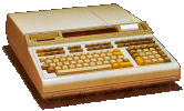
By 1972, when HP introduced the second-generation HP 9820 and 9830 desktop calculators, the Loveland Calculator Division knew that its computing machines had found a ready and growing market. It also knew that successful markets, like the market for desktop calculators, quickly draw competitors. Planning for the third-generation machines started immediately.
HP’s third-generation desktop calculators would have to be able to solve increasingly complex problems using more powerful programming languages. They would have to evolve into desktop computers. To do so, they would need faster processors and higher-capacity memories. HP Loveland’s IC facility started to develop NMOS II, the next NMOS generation.
Tom Haswell guided the overall NMOS II effort. It was Haswell who had solved the problem of gradual FET poisoning from sodium contamination in HP Loveland’s original NMOS process through a combination of pure materials, elaborate cleaning procedures, use of ultra-pure deionized water, and back-bias voltage to control threshold voltages. Haswell had developed a friendship with Tom Ligon during the original NMOS project but Ligon had left HP in 1970 to start his own business. Haswell managed to bring Ligon back to HP after his 20-month Wanderjahr. “I wasn’t really doing anything at the time.” says Ligon.
Ligon became the project leader and started working on the NMOS II process. He teamed with Joe DeWeese and, in August of that year, Ligon and DeWeese were joined by Dana Seccombe, who had just graduated from MIT. Other NMOS II contributors who joined the project after 1972 included Larry Hall (a newly minted PhD EE from the University of Wisconsin who joined HP in 1973 and who would continue to work on IC fabrication development at HP with the NMOS III team), Jim Mikkelson (who would also work on NMOS III and then go on to co-found Vitesse Semiconductor Corp. in 1984 with Louis R. Tomasetta), and Mark Lundstrom (who is now a professor of electrical and computer engineering at Purdue University, specializing in device physics and nanoscale—10nm and below—transistor technology).
As he did with HP’s first NMOS process, Dave Maitland started developing design rules for the new NMOS II process. In addition, based on his valuable experience at ISSCC in 1969 that had helped to launch Loveland’s NMOS efforts, Maitland suggested that the NMOS II development team attend future ISSCCs, starting with the one held in 1972. The NMOS II team continued to attend ISSCC for several years, which was critically important given HP Loveland’s geographic isolation from Silicon Valley, the epicenter of chip development.
Overshooting aggressive speed goals
The first goal for the NMOS II process was to double the circuit density when compared to the original NMOS chips (classical Moore’s-Law device-density doubling). The speed goal was to produce chips that were 3x faster. Ultimately, the final NMOS II process would achieve the density goal but it would wildly overshoot the speed goal. The final NMOS II chips would be 10x faster than the original NMOS ICs.
To achieve the density goal, the NMOS II process would have to use 5-μm design rules instead of the 7-μm design rules of HP’s original NMOS process. However, the existing IC-photomask technology, which employed photo emulsion on glass, could not hold the required dimensional tolerances after multiple uses. Over time, the production handling that included clamping and unclamping the masks damaged the masks. So HP switched to “hard masks,” which replaced the relatively soft photo emulsion with thin films that resisted the damage better. Initially, the thin film was made from chrome, but the shiny chrome reflected too much of the light, which caused line widths to vary. Ultimately, the NMOS II masks used thin films of silicon or iron oxide.
Not hard enough
Unfortunately, the hard masks proved unable to provide sufficient resolution for the controlled thermal diffusion of phosphorous dopant into the silicon that formed the FET sources and drains. In the early NMOS process, the wafer was prepared for diffusion by first growing a relatively thick layer of silicon dioxide, a field layer, over the entire chip. Then the field layer would be selectively removed wherever FETs were to be formed.
However, it was not possible to achieve the needed precision in lithographic resolution with this existing technique for growing the field oxide so the Loveland process engineers developed a local-oxidation process that employed a thin layer of silicon nitride as a secondary mask. First, a thin (50 Angstrom) oxide layer was grown on the silicon. This layer acted as a stress-relief layer for the nitride layer. Without this stress-relief layer, the stress caused by direct contact of the silicon and the nitride layer could cause the silicon to crack. Next, a thicker silicon nitride layer (1200-1500 Angstroms) was formed over the entire wafer, followed by depositing a thick field oxide layer (1000-1200 Angstroms). The nitride layer prevented chip-killing oxygen penetration during the oxide field growth in what would later be the active areas of the circuit.
The oxide on top of the nitride served as a photomask for the silicon nitride, which in 1970, could only be etched with a chemical etch that would also destroy the photoresist. Because the photoresist itself couldn’t be used as the actual etch mask for the nitride layer, the photo resist masked the top oxide layer, which was etched conventionally. Then the photo resist was removed and the nitride was etched using the previously etched oxide layer as the etch mask. The nitride layer was etched away except for the areas where FETs would be formed. This selective nitride etch copied the previously etched pattern from the top oxide layer to the nitride layer and formed a very thin, in-place mask for the diffusion and gate areas of the FETs. Finally, a conventional oxide etch removed the stress-relief layer, exposing the areas of the silicon that would become the FET sources and drains. The wafer was then put in a diffusion furnace, and the sources and drains were diffused with phosphorus.
Self-aligned gates
Subsequently, all the remaining oxide/nitride/oxide was removed in a maskless process and the gate oxide was grown over the wafer’s entire surface. The oxide grew over the diffusions faster than it did over the rest of the wafer because the silicon in the diffusion areas was doped with phosphorus, which encouraged oxide growth. The result was a partially self-aligned process (the gate metal would cover both the gate oxide, and part of the diffusion but, because the diffusion oxide was thicker in the diffusion region, the drain-to-gate parasitic capacitance was reduced. These self-aligned metal gates with reduced gate capacitance further increased the switching speed of the NMOS II FETs and chips beyond the speed boost from simple lithographic scaling.
Use of the silicon-nitride layer and its several additional steps increased pattern resolution—which improved device density—and reduced gate size and capacitance—which boosted chip speed. It also added significantly to the number of NMOS II fabrication steps. These additional process steps probably could not have been justified for a commercial, high-production IC fabrication process of that era because it would not have produced chips at a competitive cost. However, HP’s goals were not to create the lowest cost NMOS ICs but to produce ICs with the highest density and performance for the day. HP needed those features to ensure technological superiority in its desktop calculators, which therefore warranted the additional process steps.
Ion implantation was yet another addition to the growing number of NMOS II process steps. Some of the FETs on the NMOS II chips were doped using a particle accelerator instead of high-temperature thermal diffusion. These selected FETs needed to be precisely doped because they were used to replace load resistors in the circuits on the NMOS II chips. (FETs are smaller than on-chip resistors of the same resistance and therefore take less space on the chip.) Ion implantation partially depleted the gate regions of the FETs so that they were always switched on by a precise amount.
FETs used in this manner are called “depletion loads.” Eventually, ion implantation would replace back-gate voltage bias as an industry-wide solution to FET poisoning caused by sodium contamination, but not in NMOS II where it was mostly used to create depletion loads.
Mysterious wafer growth
|
|
|
NMOS II Process Steps
Image courtesy of the Hewlett-Packard Company
Note: This graphic has been altered from the original. Per Dana Seccombe, the
silicon nitride and silicon dioxide laters in the first graphic appeared swapped
in the original 1977 article. They appear correctly here.
|
|
The small feature sizes of the NMOS II FETs created new problems to tackle. One of these problems, unforeseen but obvious after the fact, was mysterious wafer growth during the fabrication process. Integrated circuits are fabricated using a series of many process steps. Some of these process steps involve photolithography—the exposure of patterns onto a photo-sensitized wafer through a photomask. Consequently, photomask alignment from one layer to the next is very important to the process.
With 5-μm design rules, the HP process engineers were trying to hold alignment tolerances to within 1 μm from layer to layer across the 2-inch (later 3-inch) silicon wafers and they were not succeeding. It appeared that the wafers, which much be washed frequently with pure water during the process sequence, were growing in the wash. That was clearly not possible. Silicon doesn’t absorb water so washing should not dimensionally affect the wafers.
After careful analysis of the problem, Dana Seccombe concluded that the process step that grew the field-oxide layer in the shallow wells created by selective silicon etching was causing the silicon wafers to expand because the grown silicon dioxide was pressing on the sides of the wells, which distorted the wafer and spread the previously patterned features apart just enough to exceed the desired layer-alignment tolerance. Once the problem was understood and characterized, the fix was to slightly enlarge the features on all of the photomasks that were used after the field-oxide growth step.
Short-circuited FETs
Another of the problems related to the shrinking dimensions of the NMOS II process was unwanted aluminum diffusion down through the relatively shallow (1.6 μm) doped source and drain regions in the FETs. Aluminum, which is used to interconnect FETs and other devices on the integrated circuit, alloys easily with silicon. That’s one of the main reasons it’s used for interconnection: it makes good electrical contact with the underlying silicon. (Other reasons include the fact that aluminum has excellent conductivity, it’s relatively cheap, and it’s relatively inert—for a cheap metal.) However, as the aluminum alloys with the silicon during deposition, it penetrates the silicon surface. If it penetrates too far, it travels completely through the source or drain region and short circuits the FET. In process technology terms, that’s a bad thing.
Adding silicon to the aluminum during deposition—essentially presaturating the aluminum with silicon—eliminates this problem but causes another: crystallization. The aluminum-silicon alloy tends to crystallize, which make the interconnection wires lumpy. This lumpiness can cause voids in the deposited wires, especially where they attempt to step over surface irregularities caused by the patches of silicon dioxide grown all over the chip.
|

|
|
Diffusing silicon into the aluminum interconnections on the NMOS II chips halted aluminum diffusion into the transistors, and the resulting shorts, but the added process step resulted in silicon ball crystallization. The little crystalline balls of silicon are left behind when the unwanted aluminum is etched away.
Looks bad. Works good.
Photo courtesy of Fred Wenninger
|
|
In the 21st century, this problem is solved, in part, with chemical-mechanical polishing (CMP), which creates smooth surfaces on which to deposit additional layers. But a production CMP process didn’t exist back in the 1970s. So HP’s solution to the crystallization problem was to add a little copper to the silicon-aluminum mix to make the on-chip wires more ductile. Dana Seccombe worked with Howard Abraham and Frank Ura and Steve Muto of HP Labs to develop the special planar-magnetron sputtering process needed to deposit the copper-silicon-aluminum metallization on the NMOS II chips.
The shrinking shmoo
Yet another problem that cropped up was a familiar one from the original NMOS process: on-chip current leakage due to sodium contamination. However, for NMOS II chips, the problem appeared over time instead of immediately after manufacture. NMOS II ICs fresh from the furnace would work fine, but the chips would stop working over time.
|

|
|
A Shmoo from “Li’l Abner”
|
|
None of the measureable test devices patterned on the early NMOS II chips tested bad initially, but high-temperature testing predicted early chip failures because the chips’ shmoo plots shrank during these accelerated life tests. A shmoo plot—named for their resemblance to small, edible, and very delicious creatures in the old “Li’l Abner” comic strip created by Al Capp—shows the operating region of a chip over a range of operating temperatures and voltages. Process engineers want to see as big a shmoo as possible to ensure that the chip will work over a wide range of operating conditions. A shmoo that shrinks during accelerated life tests indicates that a chip will most likely die, as its shmoo vanishes.
The culprit in the shrinking-shmoo problem turned out to be the silicon-dioxide passivation layer, the topmost layer on the NMOS II chips. This layer is supposed to stop contamination such as sodium ions from getting into the chip’s lower layers but this layer was not doing its job. It was allowing sodium ions to enter the active regions of the NMOS II chips, which poisoned and eventually killed the FETs over time.
In fact, it was likely that the passivation layer itself was contaminated with sodium so adding the passivation layer probably exacerbated the contamination problem. Heat accelerates the problem’s appearance by increasing the mobility of the sodium ions so that they penetrate the chip faster. Hence the shrinking shmoo plots over the course of the accelerated NMOS II life tests.
|
|
|
Bob Watson
Photo courtesy of the
Hewlett-Packard Company
|
|
|
|
Henry Kohoutek
Photo courtesy of the
Hewlett-Packard Company
|
|
Dana Seccombe and Larry Hall worked on this problem and their solution consisted of using high-temperature glass passivation, adding phosphorous doping to the passivation layer, and adding a silicon-nitride cap layer on top of the glass passivation. These steps improved the passivation’s imperviousness to ionic contamination and the added phosphorous doping acted as a “getter” that trapped any sodium ions that subsequently infiltrated the passivation layer (or that got in during the layer’s creation). The getter prevented the sodium ions from migrating into the transistor’s gates and poisoning the operating FETs. The new, improved passivation process stopped the shrinking shmoos.
Release to production: a shotgun wedding
With the shrinking-shmoo problem fixed, NMOS II was ready for production. Whenever a product becomes ready for production, HP held a release-to-production meeting. This meeting resembles a wedding between the manufacturing department and the new product. The R&D Lab gives the new product (the bride) away to the manufacturing department (the groom). In particular, there’s a part of the wedding where the officiator says “If anyone here knows of any reason why these two should not be wed, let them speak now or forever hold their peace.” At a release-to-production meeting, the heads of various departments are given the chance to prevent the release by objecting for various reasons.
At the NMOS II release-to-production meeting, R&D lab manager Bob Watson asked process engineer Dana Seccombe if the NMOS II process was ready for production. On the basis of his new, non-shrinking shmoos, Seccombe said, “Yes.” Henry Kohoutek, the quality manager at the time, then spoke up. “I don’t believe you,” he said, thus objecting to the wedding. Kohoutek was not swayed by Seccombe’s accelerated life-test data and wanted to see successful long-term operation of NMOS II chips before he’d be a believer. Watson then asked again, “Do we ship?” Seccombe again said, “Yes.”
Bad day for a ROM failure
Kohoutek was overruled, the NMOS II chips shipped, and they worked in HP’s production machines.
With one key exception.
As the HP 9825A was being readied for production, HP brought the press in for a preview. Unfortunately, the demo machine was loaded with ROMs that had shrinking shmoos. One version of Murphy’s Law states that anything that can go wrong, will go wrong ... at the worst possible time. Of course, one of the bad ROMs did fail, bringing the press demo to an abrupt halt until a replacement machine could be wheeled in.
The shrinking-shmoo problem also created a boon for the Loveland Calculator Division’s R&D lab. It produced batches of “short-lived” operating-system ROMS for the engineers in the R&D labs who needed operational HP 9825A desktop computers before full NMOS II production commenced. Several engineers swiped some early ROMs and populated a blank language-ROM board with these out-of-spec parts. These language-ROM boards worked for about a year and then died but by then, full-spec ROMs with improved passivation were available.
References:
Information about the development of the NMOS II process came from personal discussions with Dana Seccombe and Tom Ligon and from:
Joseph E DeWeese and Thomas R Ligon, “An NMOS Process for High-Performance LSI Circuits,” HP Journal, November, 1977, p 26-32.
|
|